Loofbourrow · Volume 5
Steering & the Analog Control Front-End
5.1 Steering
5.1.1 The separate steering motor
Microtron’s front wheel does not share a motor with the two rear drive wheels. A dedicated steering motor — mounted at the apex of the triangular chassis — pivots the front wheel independently of the propulsion function. As documented in Vol. 3, Diagram A of the Interface Age article labels this element “Steering Motor with gear,” confirming both the separate motor and the presence of a gearing arrangement at the wheel pivot (Interface Age, Apr. 1977, Diagram A).
The front wheel is simultaneously a motorized drive wheel and the robot’s sole steerable element: it contributes propulsive force in common with the fixed rear wheels while being swept through an angular range to govern the turning arc of the chassis. The steering range spans 0° to 60° (cyberneticzoo). The steering motor’s manufacturer, part number, and electrical ratings are not stated in the available primary sources and are not claimed here.
5.1.2 The gear reduction
The Interface Age article records that the steering motor, when initially connected to the front-wheel pivot, turned the wheel far faster than any useful steering maneuver required (Interface Age, Apr. 1977). Loofbourrow resolved this by introducing a gear reduction between the motor shaft and the wheel pivot: a large gear fitted to the front-wheel shaft meshes with a small gear on the steering-motor shaft. With the larger gear on the driven side and the smaller gear on the driving side, the angular velocity delivered to the wheel is reduced relative to the motor output, and the available torque at the wheel pivot increases proportionally (Interface Age, Apr. 1977). The exact tooth counts of both gears and the resulting numerical speed-reduction ratio are not stated in the article and are not claimed here.
5.1.3 Steering Motor Control — Diagram C (continued)
Diagram C of the Interface Age article spans two schematic sections. The first — “Motorized Wheel Control” — covers the drive-wheel motor circuit and is documented in Vol. 4. The second section, captioned “Steering Motor Control,” presents the circuitry that energizes the steering motor in the correct direction in response to “Steer Left” and “Steer Right” command signals from the KIM-1.
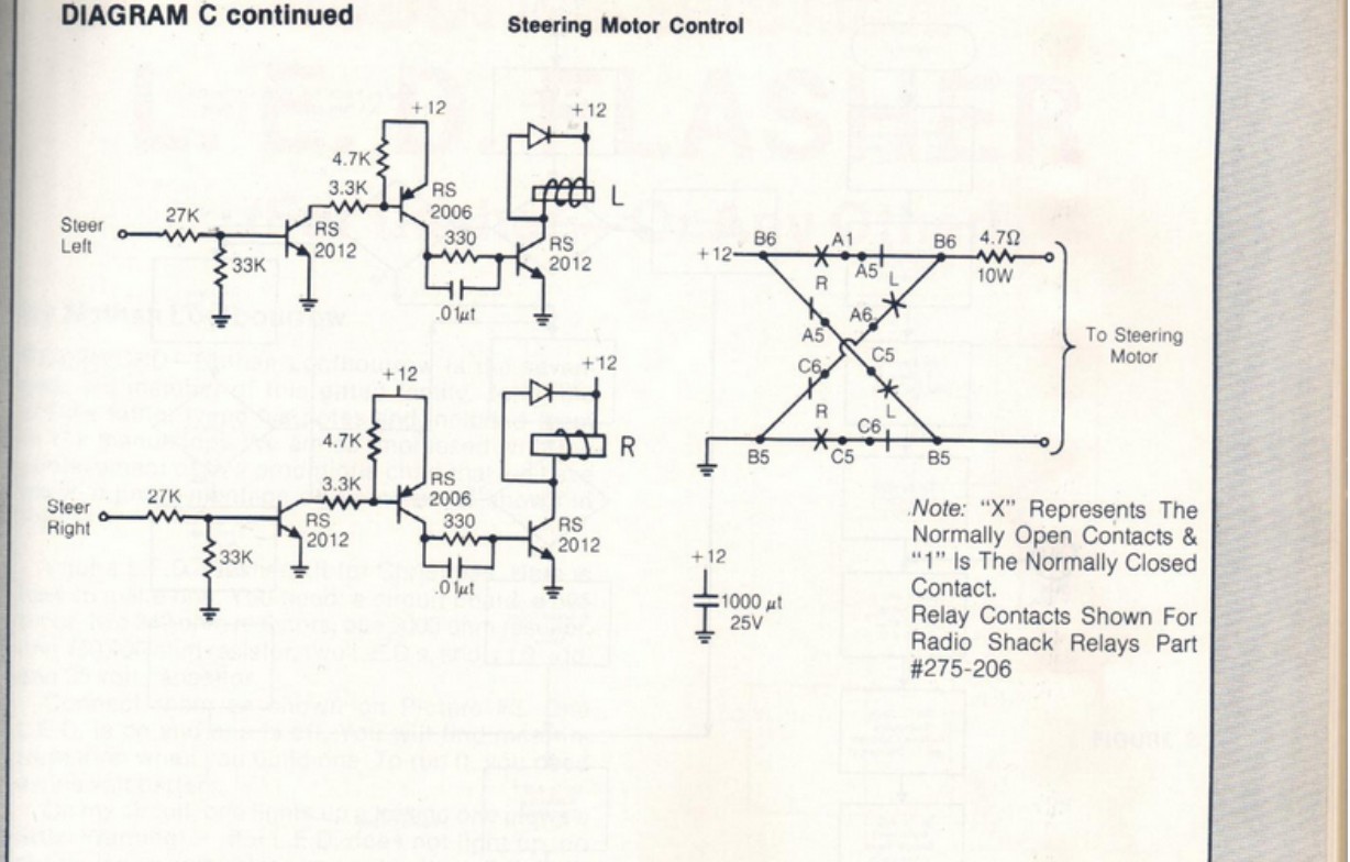
5.1.3.1 Component labels read from the scan
The following components are labeled in the diagram. Part designations are transcribed as read from the scan; ambiguities are flagged where the image introduces a genuine reading risk.
Table 1 — Component labels read from the scan
| Component | Label as read | Reading notes |
|---|---|---|
| Input series resistors | 27K (×2) | One per driver chain; reads clearly |
| Pull-down resistors | 33K (×2) | One per driver chain; reads clearly |
| Small-signal transistors | RS 2012 (multiple per chain) | Two instances per chain — input stage and output stage; “RS” prefix consistent with Radio Shack part designation |
| Intermediate driver transistors | RS 2006 (×2) | One per chain; reads clearly; the same device used in the drive circuit’s intermediate stage (Vol. 4) |
| Intermediate-stage biasing resistors | 3.3K, 4.7K (×2 sets) | Pull-up network for the RS 2006 stage in each chain |
| Output-stage base resistors | 330Ω (×2) | Reads clearly in both chains |
| Bypass capacitors | Read as “.01μt” per chain | Small bypass caps at the driver output stage; scan resolution introduces genuine ambiguity between 0.01 μF (10 nF) and 0.1 μF (100 nF); this value should be verified against a cleaner scan before treating as definitive |
| Relay coils | L (Steer Left relay coil), R (Steer Right relay coil) | Each coil driven by its respective RS 2012 output transistor |
| Flyback protection diodes | Unlabeled (×2) | One across each relay coil; polarity visible in diagram; part numbers not given |
| Motor series resistor | 4.7 Ω 10 W | In the “To Steering Motor” output path; reads clearly |
| Supply decoupling capacitor | 1000 μF 25 V | On the +12 V rail entering the relay contact section |
| Relay part number | Radio Shack Part #275-206 | Stated verbatim in the diagram’s own note; no scanning ambiguity in this designation |
| Supply rail | +12 V | Motor supply and relay-coil supply throughout the steering circuit |
No HEP-designated transistors appear in this portion of the diagram. The HEP S0019 and SK 3036 devices documented in Vol. 4 are confined to the drive-wheel side of Diagram C; the steering driver uses only RS 2012 and RS 2006 devices.
5.1.3.2 Circuit topology
The two driver chains are structurally identical and operate independently. Each begins with a logic-level signal — Steer Left or Steer Right, sourced from the 7404 inverter described in the Power section below — applied through a 27 K series resistor with a 33 K pull-down to ground. This voltage divider scales the incoming logic level to a safe base drive for the first RS 2012 transistor. That transistor drives an RS 2006 through a 3.3 K and 4.7 K biasing network, and the RS 2006 in turn drives a second RS 2012 through a 330 Ω base resistor. The final RS 2012 sinks current through the relay coil, energizing it when the corresponding steer signal is asserted. A flyback diode across each coil protects the output transistor from inductive back-EMF when the relay releases.
The two relays together form a crossover contact matrix that determines the polarity of current through the steering motor. The diagram’s own note defines the notation: “X” represents normally-open contacts and “1” represents the normally-closed contact for the Radio Shack 275-206 relay. When neither relay is energized the motor is at rest; when the Steer Left relay fires, current flows through the motor in the left-turn polarity; when the Steer Right relay fires, the polarity reverses and the motor drives the wheel toward the right. A 4.7 Ω 10 W resistor in the motor output path provides current limiting; the 1000 μF 25 V bulk capacitor on the +12 V supply absorbs inductive transients from relay switching. The characterization of this crossover arrangement as a relay-based polarity reverser is general engineering context and is not attributed to the article.
5.2 Reading the operator: the comparators
5.2.1 The bridge from analog to digital
The operator commands Microtron’s speed and steering through potentiometers and joystick-type controls. These produce continuously variable analog voltages. The KIM-1’s 6502 reads logic levels on its port-A (PA) lines — each bit is either high or low. Diagram D of the Interface Age article shows the circuit that bridges this gap: a set of operational-amplifier comparators that compare the analog voltages from the operator’s pots against reference levels derived from additional resistive dividers, and produce digital logic outputs that the KIM-1 can read through specific pins on the microprocessor connector.
This is the robot’s analog front-end. Its digital outputs drive the PA input lines that the 6502’s assembly routines poll to determine operator intent; the speed-control and steering software responds to those pin states. The assembly routines, polling addresses, and branching logic are examined in Vol. 7.
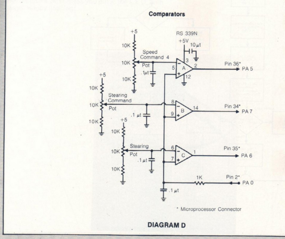
5.2.1.1 Component labels read from the scan
Table 2 — Component labels read from the scan
| Component | Label as read | Reading notes |
|---|---|---|
| Comparator chip | RS 339N | Reads clearly at upper right of the diagram; “RS” prefix is consistent with Radio Shack sourcing; “339N” matches the part number of the widely used LM339N quad comparator — an open-collector output, single-supply-capable device (general context; not attributed to the article). The RS 339N is treated throughout this volume as Radio Shack’s stocked designation for this quad comparator |
| Chip supply decoupling | +5 V, 10 μF | Reads clearly at the supply pin |
| Voltage-divider resistors | 10K (all) | Six instances visible — two per active comparator input path; all read consistently |
| Input bypass capacitors | 0.1 μF | One per active comparator stage; labeled “.1μt” or “0.1μt” in the scan (= 100 nF) |
| PA 0 path series resistor | 1K | In the separate filtered path to Pin 2 / PA 0 |
| PA 0 path bypass capacitor | 0.1 μF | In the same PA 0 path |
| Supply rail | +5 V | All comparator and divider circuitry referenced to this rail |
5.2.1.2 Comparator-to-PA-pin assignments
Each of the three active comparator stages drives one KIM-1 port-A input through the microprocessor connector. The assignments read from Diagram D are consistent with the table documented in Vol. 2:
Table 3 — Each of the three active comparator stages drives one KIM-1 port-A input through the microprocessor connector. The assignments read from Diagram D are consistent with the table documented in Vol. 2
| Comparator | Labeled operator input | Output → Connector pin | Port-A pin |
|---|---|---|---|
| A | Speed Command 4 / Pot | Pin 36 | PA 5 |
| B | Steering Command Pot | Pin 34 | PA 7 |
| C | Steering Pot | Pin 35 | PA 6 |
A note on the “Speed Command 4” label: Diagram D labels the upper input to comparator A as “Speed Command 4.” The numeral 4 appears in the diagram without explanation in the available primary source; its significance — whether it denotes a speed level, a pot-index number, or a schematic reference — is not interpreted here. The label is transcribed exactly as it appears in the diagram.
The polarity sense of each comparator stage — which input is connected to the inverting terminal and which to the non-inverting terminal — cannot be determined with certainty from the scan resolution alone and is not asserted here.
PA 0 / Pin 2. At the bottom of Diagram D, a 1K series resistor and a 0.1 μF bypass capacitor connect a node in the Steering Pot section of the circuit to Pin 2 / PA 0 on the microprocessor connector. Unlike the three paths above, no comparator triangle symbol appears between the pot network and this connection in the diagram. The nature of this signal — whether it carries a filtered analog reference, a logic level from a circuit element not visible in the available scan, or some other function — is not labeled in Diagram D and is not claimed here.
5.2.1.3 How a comparator digitizes a pot voltage (general context)
An op-amp comparator compares two voltages and switches its output to a logic high or logic low depending on which input is larger. In the Diagram D configuration, each active comparator stage compares the wiper voltage of an operator-controlled pot against a reference derived from the resistive dividers and a second pot. As the operator sweeps the control pot through its range, the voltage at one comparator input rises past the reference voltage, toggling the comparator output and changing the logic level seen at the corresponding KIM-1 PA bit. The 6502 assembly routines read these PA bits as one-bit flags — each bit state signals whether a particular speed or steering threshold has been crossed. The RS 339N’s open-collector outputs require pull-up resistors to the logic supply to produce valid high levels; those pull-up resistors are visible in Diagram D as the 10K elements at the comparator inputs. This description of comparator function is general electronics context and is not attributed to the Interface Age article. The specific threshold voltages implied by the pot and divider values, and the number of discrete conditions encoded by the full set of PA bits, are examined in Vol. 7 in connection with the assembly listings.
5.3 Power
5.3.1 Diagram B: Power Supply and Inverters
Diagram B of the Interface Age article covers two subsystems on the same diagram page: the main power supply, which distributes 12 V battery voltage and generates regulated 5 V logic rails; and an inverter section, which adapts the KIM-1’s port-A output bits into motor-command signals suitable for driving the base networks of the transistor chains in the drive and steering circuits.
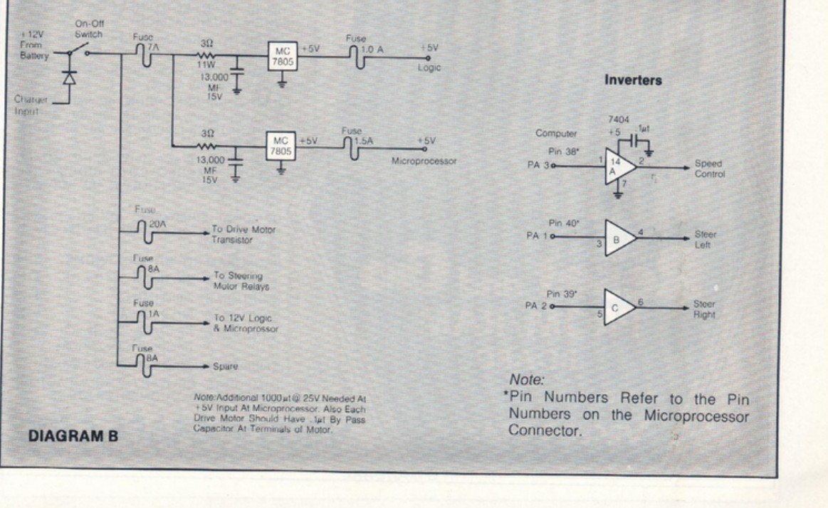
5.3.2 The 12 V distribution network
The primary energy source is a 12 V automotive battery housed inside the triangular aluminum frame (Vol. 3, Diagram A). Diagram B shows the battery voltage entering through an on/off switch; a separate charger-input connection is also shown, permitting the battery to be recharged without removal from the chassis (Interface Age, Apr. 1977). A 7 A fuse appears at the input to the regulated supply section.
From the common supply bus, individually fused branches distribute +12 V to each load:
Table 4 — From the common supply bus, individually fused branches distribute +12 V to each load
| Branch | Fuse | Destination |
|---|---|---|
| Drive motor | 20 A | To Drive Motor Transistor (SK 3036 — Vol. 4) |
| Steering motor | 8 A | To Steering Motor Relays (Diagram C steering, above) |
| 12 V logic and microprocessor | 1 A | To 12 V logic circuits and the KIM-1 |
| Spare | 8 A | Unassigned reserve branch |
The 20 A drive-motor fuse is consistent with the catalog wheel rating of 8 A stall current per wheel, with three wheels producing a potential aggregate stall draw documented in Vol. 4. The 8 A fuse for the steering motor relays covers the relay coil currents and the steering motor load; the steering motor’s own current rating is not stated in the available sources and is not claimed here.
5.3.3 Regulated 5 V rails
Two MC 7805 three-terminal positive-voltage regulators produce the 5 V logic supply (Interface Age, Apr. 1977, Diagram B). The part designator “MC 7805” reads clearly in the scan — “MC” is Motorola’s house prefix for this industry-standard device. Each regulator is preceded by a 3 Ω series resistor and an input filter capacitor labeled 13,000 μF at 15 V; the series resistor reduces the input-to-output differential at the regulator and therefore its internal power dissipation (general context; not attributed to the article). Two separate regulated outputs serve distinct loads:
Table 5 — Two MC 7805 three-terminal positive-voltage regulators produce the 5 V logic supply (Interface Age, Apr. 1977, Diagram B). The part designator "MC 7805" reads clearly in the scan — "MC" is Motorola's house prefix for this industry-standard device. Each regulator is preceded by a 3 Ω series resistor and an input filter capacitor labeled 13,000 μF at 15 V; the series resistor reduces the input-to-output differential at the regulator and therefore its internal power dissipation (general context; not attributed to the article). Two separate regulated outputs serve distinct loads
| Regulated rail | Output fuse | Destination |
|---|---|---|
| +5 V Logic | 1.0 A | General +5 V logic circuits |
| +5 V Microprocessor | 1.5 A | KIM-1 board and microprocessor-connector circuits |
Providing separate regulated rails isolates the KIM-1’s supply rail from switching transients generated by the relay and transistor circuits on the same chassis. Diagram B includes two printed notes: that an additional 1000 μF at 25 V is needed at the +5 V microprocessor input, and that each drive motor should have a 0.1 μF bypass capacitor at its terminals. Both notes appear verbatim in the diagram and are attributed to it.
5.3.4 The 7404 inverter stage
The right side of Diagram B, labeled “Inverters,” shows three gates of a 7404 hex-inverter package powered from +5 V with a 1 μF decoupling capacitor. Three KIM-1 port-A output lines drive the inverter inputs; the 7404’s inverted outputs become the Speed Control, Steer Left, and Steer Right signals that enter the motor-driver circuits. The connections read from Diagram B are:
Table 6 — The right side of Diagram B, labeled "Inverters," shows three gates of a 7404 hex-inverter package powered from +5 V with a 1 μF decoupling capacitor. Three KIM-1 port-A output lines drive the inverter inputs; the 7404's inverted outputs become the Speed Control, Steer Left, and Steer Right signals that enter the motor-driver circuits. The connections read from Diagram B are
| KIM-1 PA pin | Microprocessor connector pin | 7404 output signal |
|---|---|---|
| PA 3 | Pin 38 | Speed Control |
| PA 1 | Pin 40 | Steer Left |
| PA 2 | Pin 39 | Steer Right |
Speed Control drives the SK 3036 power-transistor chain in the drive circuit (Vol. 4, Diagram C). Steer Left and Steer Right drive the corresponding RS 2012 / RS 2006 transistor chains in the steering circuit above, energizing the appropriate relay to commutate the steering motor. The 7404 inverts each KIM-1 output before it reaches the transistor base networks; the 27 K / 33 K bias resistors in both the drive and steering chains are therefore sized for the 7404 output level rather than for direct KIM-1 port drive. The specific reason for the inversion — whether it matches an active-low transistor-base convention, reflects a polarity choice in the assembly code, or serves another purpose — is not stated in the available primary source and is not claimed here.
The pin labels visible in Diagram B for the 7404 are consistent with a standard 14-pin DIP 7404 hex-inverter package (general context). The diagram explicitly labels VCC at pin 14 and shows the +5 V decoupling at that point; GND at pin 7 is implied by the circuit. Internal gate pin numbers are not asserted beyond what the diagram itself labels.
5.3.5 The complete signal path
With all three diagrams assembled, the end-to-end chain from operator input to motor action is:
- The operator moves a potentiometer or joystick, producing an analog voltage.
- Diagram D comparator stages compare that voltage against reference levels; each comparator output switches the logic level seen at one KIM-1 PA input pin — PA 5 (Pin 36), PA 7 (Pin 34), PA 6 (Pin 35), and via the separate 1K-filtered path, PA 0 (Pin 2).
- The 6502, executing the assembly routines stored in the KIM-1’s 1 KB of RAM, polls those PA input bits and determines which speed and steering thresholds have been crossed.
- The 6502 asserts the appropriate PA output bits: PA 3 (Pin 38) for speed, PA 1 (Pin 40) for steer left, PA 2 (Pin 39) for steer right.
- The 7404 inverters in Diagram B buffer and invert those bits into the Speed Control, Steer Left, and Steer Right logic signals.
- Speed Control enters the Diagram C drive-circuit transistor chain, controlling the SK 3036 that governs drive-motor current. Steer Left and Steer Right enter the Diagram C steering transistor chains, energizing the appropriate relay and commutating the steering motor in the selected direction.
The 6502 assembly code that performs step 3 — polling sequences, speed-table lookups, steering thresholds, and the full assembly listings — is the subject of Vol. 7.
Comments (0)